← Mega 2560 Pro Mini Schematic: Master Your Arduino Projects! Arduino mega 2560 pro: pinout guide and schematics Pencil Drawing Landscapes – Stunning Examples You Must Try! How to draw a landscape with a pencil : how to draw and shade a scenery →
If you are looking for lvds interface conversion to mipi interface, resolution up to 1920x1200 you've visit to the right page. We have 25 Pictures about lvds interface conversion to mipi interface, resolution up to 1920x1200 like LVDS: High Speed LVDS PCB Design Guidelines | MADPCB, FPGA - DAC LVDS 1.25GBPS PCB SKEW IMAGE - YouTube and also LVDS: High Speed LVDS PCB Design Guidelines | MADPCB. Here you go:
Lvds Interface Conversion To Mipi Interface, Resolution Up To 1920x1200
 lcddisplay.co
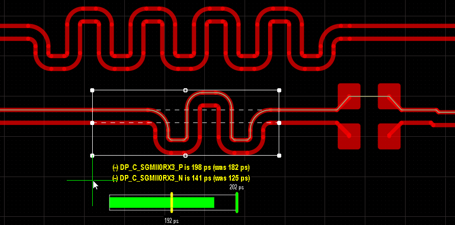
PCB Trace Length Matching Guidelines - TechSparks
 www.tech-sparks.com
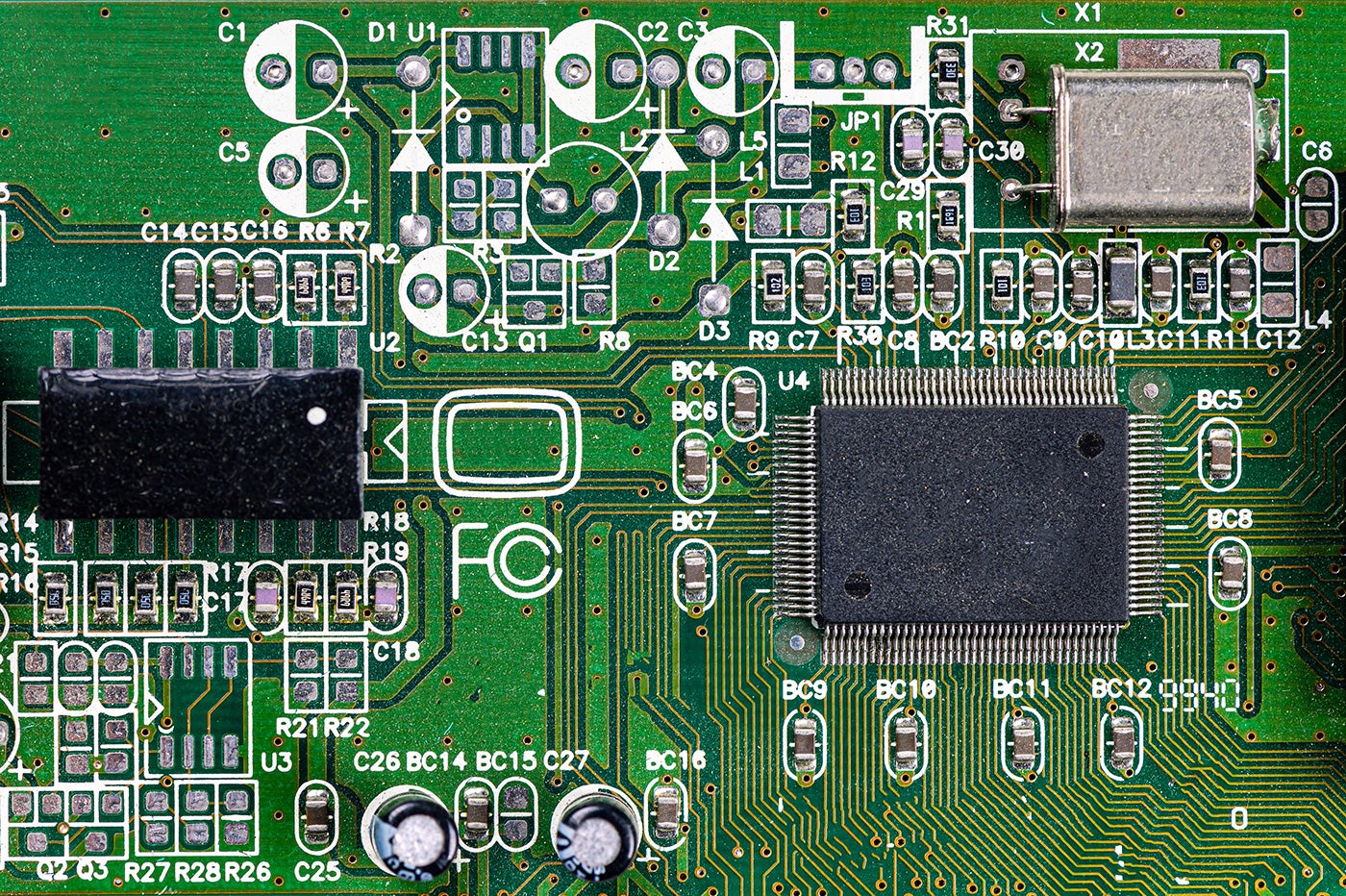
Main Design Guidelines & Layout Rules On High Speed PCB
 www.integrasources.com
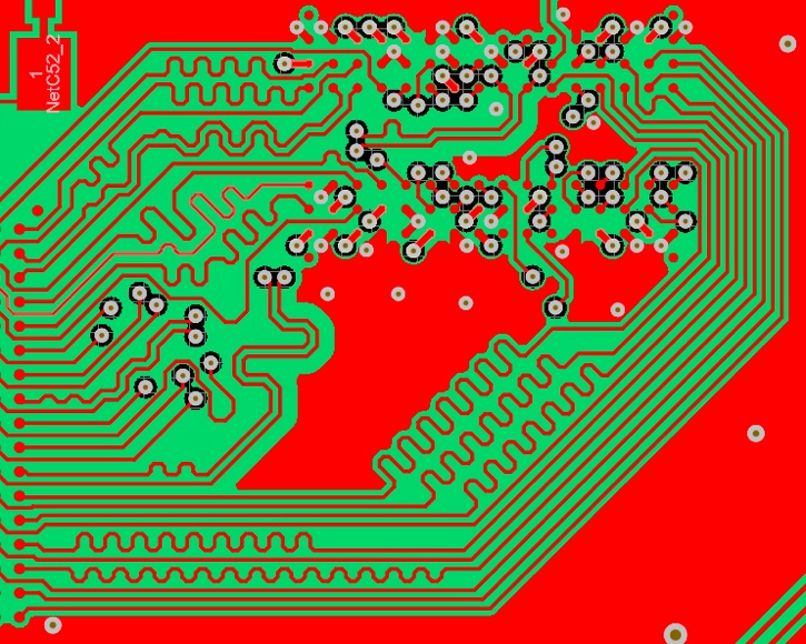
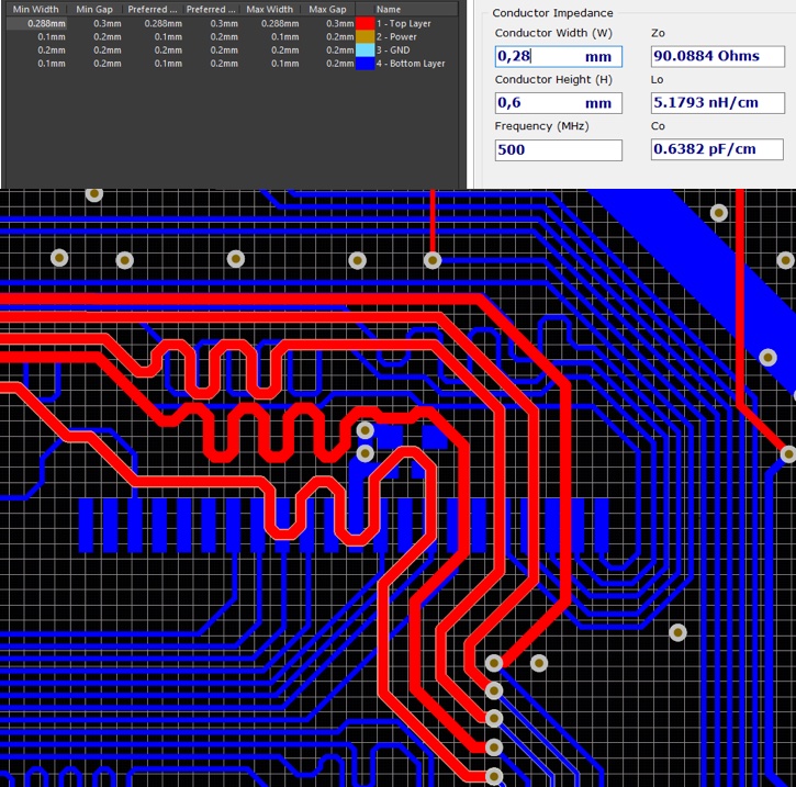
Some LVDS PCB Layout Guidelines For Ensuring Signal Integrity | PCB
 resources.altium.com
lvds pcb ensuring integrity altium buffer levels voltage physical
Some LVDS PCB Layout Guidelines For Ensuring Signal Integrity | PCB
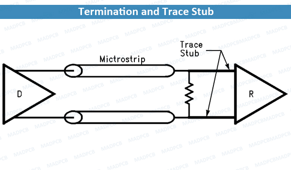
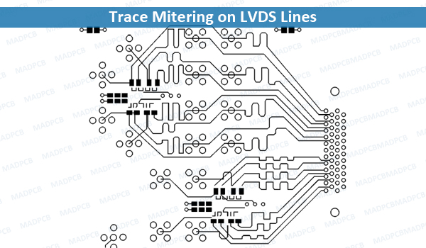
LVDS: High Speed LVDS PCB Design Guidelines | MADPCB
 madpcb.com
FPGA - DAC LVDS 1.25GBPS PCB SKEW IMAGE - YouTube
 www.youtube.com
pcb lvds fpga skew
Some LVDS PCB Layout Guidelines For Ensuring Signal Integrity | PCB
 resources.altium.com
LVDS: High Speed LVDS PCB Design Guidelines | MADPCB
 madpcb.com
A Detailed Guide To PCB Layout Design - IBE Electronics
 www.pcbaaa.com
Some LVDS PCB Layout Guidelines For Ensuring Signal Integrity | PCB
 resources.altium.com
Main Design Guidelines & Layout Rules On High Speed PCB
 www.integrasources.com
PCB Layout Efficiency: Tools To Optimize Your Design | EMA Design
 www.ema-eda.com
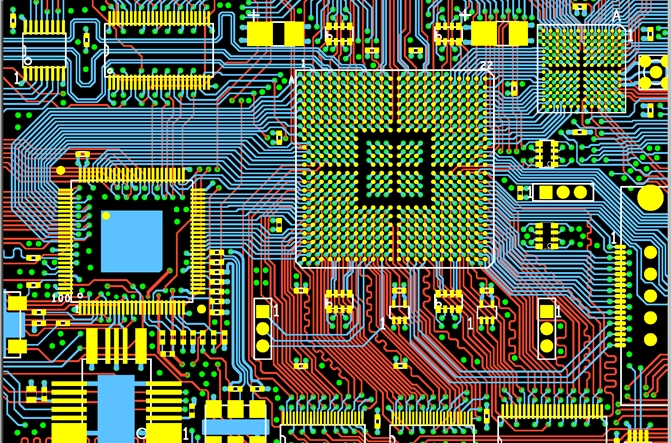
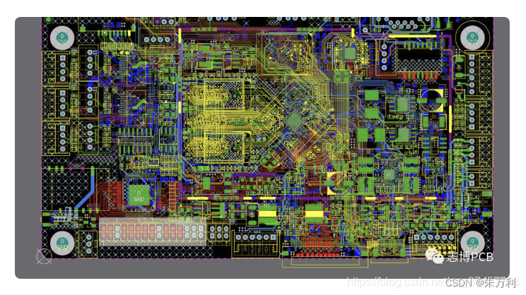
PCB模块化设计12——LVDS高速PCB布局布线设计规范_22pin接口模块设计-CSDN博客
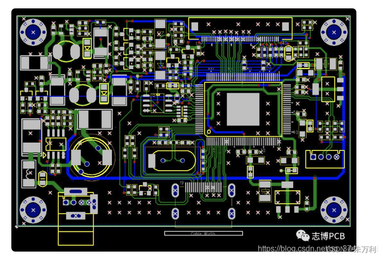 blog.csdn.net
24. Top 5 PCB Design Guidelines Every PCB Designer Needs To Know,PCB Design
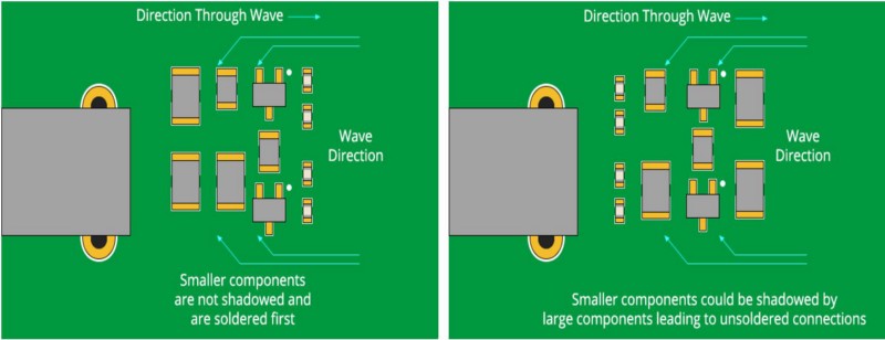 www.juvtmall.com
placement pcb design component guidelines good components poor assembly needs designer every know top left right circuits
Some LVDS PCB Layout Guidelines For Ensuring Signal Integrity | PCB
PCB Design Guidelines For High Current Applications - HardwareBee
 hardwarebee.com
pcb design layout guide high guidelines electronic ultimate process
How LVDS PCB Layout Guidelines Affect Signal Integrity | Cadence System
 www.linkedin.com
An Ultimate Guide To Pcb Wiring And Layout - Vrogue.co
 www.vrogue.co
Pcb Design Layout Guidelines Pcb Layout Guidelines For Design 21+ Pcb
 pcbhouse.pages.dev
Pcb Design Differential Impedance Of Lvds Rules And T - Vrogue.co
 www.vrogue.co
Main Design Guidelines & Layout Rules On High Speed PCB
 www.integrasources.com
PCB模块化设计12——LVDS高速PCB布局布线设计规范_22pin接口模块设计-CSDN博客
 blog.csdn.net
LVDS: High Speed LVDS PCB Design Guidelines | MADPCB
 madpcb.com
LVDS: High Speed LVDS PCB Design Guidelines | MADPCB
 madpcb.com
Some lvds pcb layout guidelines for ensuring signal integrity. Some lvds pcb layout guidelines for ensuring signal integrity. Pcb design differential impedance of lvds rules and t